What is a Semiconductor Test Board (ATE)?
ATE, the full name of Automated Test Equipment, is a device that automatically tests the function and performance of wafers and chips after packaging. ATE equipment can perform parameter testing, functional testing, performance testing, fault detection, reliability testing, etc. of chips, and play a crucial role in the semiconductor manufacturing process.
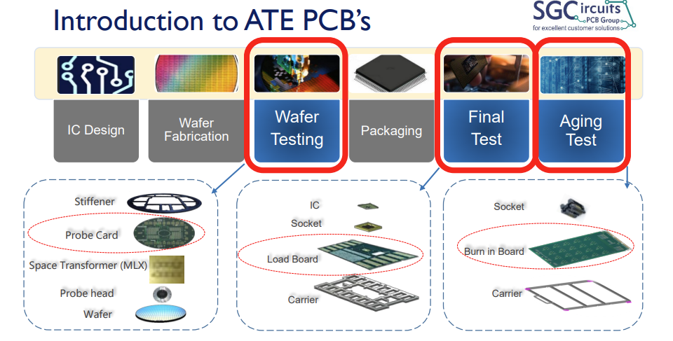
Probe Card: The probe card is used to test uncut and unpackaged semiconductor devices, and by conducting electrical tests on each chip on the wafer, the parameters within the required range are screened out for packaging.
Load Board: The load board is used on the Final Test test equipment, which is used to test the function or performance of the device after the device is packaged, and to screen out the defective device after packaging. For ICs with high-speed interfaces, the corresponding load board usually has strict impedance requirements.
Burn-in Board (BIB): Burn-in board (BIB) is used for burn-in testing of post-packaged chips, such as thermal cycling or accelerated switching cycles, to expose early failure failures of the device. The PCB material of the aging board must be able to withstand prolonged and repeated exposure to high-temperature environments with extreme reliability.
PCB processing requirements for ATE boards
As integrated circuits (ICs) become smaller and more complex, so does the density and complexity of ATE test boards.
Alignment accuracy and high aspect ratio
The number of layers of the load board is usually more than 30 layers, the BGA pitch is usually 0.35 to 0.5mm, the drill-to-conductor distance is less than 4mil, and the parallel test channels: 4 sites, 8 sites, to 16 sites. Higher requirements are put forward for PCB layer alignment, drilling accuracy, copper plating under high thickness-to-diameter ratio, and resin plugging processes.
Ultra-high-density test interface
The pitch of BGA on Probe Card is usually between 85~200um, and high-end products will be between 40~55um. If the line exceeds the PCB process capacity, it is necessary to use the MLO/MLC adapter board of the packaging substrate process and test it after the transfer.
flatness
The PCB of probe card and high-end ATE has high requirements for flatness, and the warpage rate should be controlled within 0.1%~0.2%. The height difference of the pad in the BGA area should be kept within 50um (2mil), and the required range should be kept within 25~28um (1mil) when it is stricter.
Appearance quality
Since the unit under test (DUT) area is connected to the pad by a probe, the pad must not be dented or damaged, and the pad metal surface must not have scratches or roughness issues.
Signal integrity
High-end ATE plates require impedance tolerances of ±5% and stub lengths of 8 to 12 mils or less, which require strict impedance requirements for coating, etching uniformity, and back-drilling process capabilities.